Manufacturing and inspection equipment
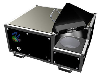
PL mapper
Manufacturing and inspection equipment
PL mapper
Photoluminescence and film thickness mapping and measuring system for LED/LD production (for 2, 3, 4, and 6 inch wafers)
Main unit specifications
| Basic model | YWAFER- GS6 | YWAFER- GS6-RT | YWAFER- GS6-R | YWAFER- GS6-PL |
|
|---|---|---|---|---|---|
| Optical range and sensitivity model list |
UVVIS; 280~850nm VISNIR; 350~1030nm UVNIR; 200~1100nm NIR; 900~1600nm (Far-red light supported cooling InGaAs detector) 540NIR; 540~1100nm (High sensitivity to red light)) UVNIR-HISENS; 200~1100nm (High sensitivity to ultraviolet light) |
||||
| Supported wafer sizes | 2, 3, 4, and 6 inch GS6-RDHLD; 1/4 cut wafer tray (optional) GS6-2.5HLD; 2.5 inch wafer tray (optional) GS6-2x3HLD; 2 inch wafer x 3 corresponding trays (optional) |
||||
| Wafer transfer | Manual | ||||
| Mapping intervals | 0.04mm~(0.1mm precision) | ||||
| Measurement using transmitted light | Measurement items | Average transmission coefficient Film thickness (converted into GaN film thickness) |
Not available | ||
| Precision / reproducibility |
Within 1% (for GaN film between 0.5 and 50μm) / within 10 nm | Not available | |||
| Measurement using reflected light | Measurement items | Not available | Average reflectance Film thickness (converted into GaN film thickness) Surface roughness / dispersion DBR (distribution Bragg reflector) characteristics |
Not available | |
| Precision / reproducibility |
Not available | Within 1% (for GaN film between 0.5 and 50μm) / within 10 nm | Not available | ||
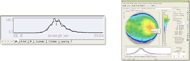
| Photoluminescence (PL) measurement |
Measurement items | Peak wavelength / Relative integrated intensity / Relative peak intensity / Half bandwidth (FWHM) / Dominant wavelength (CIE wavelength) | |||
| Wavelength resolution | – 0.3 nm (Note: – 0.7 nm for UVNIR-HISENS; – 2.0 nm for NIR) | ||||
| Light intensity precision | 3% (Relative peak intensity / Relative integrated intensity, when the YWafer intensity calibration function is used) | ||||
| Peak wavelength repeatability | < 1 nm (Peak wavelength / Half bandwidth) | ||||
| Minimum half bandwidth | – 1.5 nm | ||||
| Types of PL pumped lasers (up to four units) |
266 nm, 325 nm (external, with optical fiber), 375 nm, 405 nm, 532 nm; Contact us for other types. | ||||
| Control | Connection interface | PC-based USB / Digital I/O | |||
| User interface / Language | PCs with Microsoft Windows ™ XP / Japanese or English (user’s choice) | ||||
| Other options | GS-SPCFLT : Light attenuation and wavelength filter control GS-LASFLT : Laser intensity filter control GS-CUSTHLD : Custom sample tray GS-TURBOSCAN : High-speed scanning supported (only for PL measurement) |
||||
Software
| Version | YWaferController v3.06 |
|---|---|
| Program language | Multithreaded Visual C++ |
| Operation mode | Operator, engineer, maintenance |
| Feature | Spectral analysis with high repeatability, eliminating effects of internal interferences |
Performances
| Processing timer per wafer | Manual wafer loading/unloading | -20 sec (operator dependent) | |
|---|---|---|---|
| Measurement of reference values (for correcting values) | < 4 sec | ||
| Reference: When 2-inch wafers are measured (min: sec) | |||
| Normal | High speed (optional) | ||
| 0.5 mm intervals (measurement of 7429 points) | 7:55 | 3:26 | |
| 1.0 mm intervals (measurement of 1868 points) | 2:34 | 1:02 | |
| 2.0 mm intervals (measurement of 468 points) | 0:51 | 0:31 | |
Handling specifications (main unit)
| Operating/installation environment | Place | Inside a clean room (class 1,000 – 10,000) |
|---|---|---|
| Temperature | 15 – 35♀ | |
| Humidity | < 85%RH (no condensation) | |
| Dimensions | (L) 540 x (W) 640 x (H) 300 mm | |
| Weight | 40 kg | |
| Input voltage | AC 100~240 V 50/60 Hz | |
| Power consumption | 120 W or below | |
Other Manufacturing and testing equipment & parts products
- YSystems PL mapper
- Alphax LD testing and sorting system
- Four Technos die bonder
- Four Technos wire bonder
- Alphax LD temperature characteristic testing system
- FTD alignment and welding system
- Nippon Seisen Semiconductor Gas Filter [NASclean®]
- Pressure Transmitter – Tem Tech Lab
For inquiries about Manufacturing and inspection equipment for laser diodes
For inquiries about our products and business negotiations
Contact by formContact by phone
+81-(0)3-6412-6032